原子层沉积(ALD)
原子层沉积(ALD)是一种薄膜生长技术,能够为电子器件(电源和射频)沉积无针孔和均匀的绝缘体薄膜。ALD在高长宽比沟槽和通孔结构上提供了优异的保形性,在角级的厚度控制,以及基于连续、自限性反应的可调整薄膜成分。Samco提供高度灵活的开放式热ALD系统AL-1和负载锁定等离子体增强ALD系统AD-230LP。
-
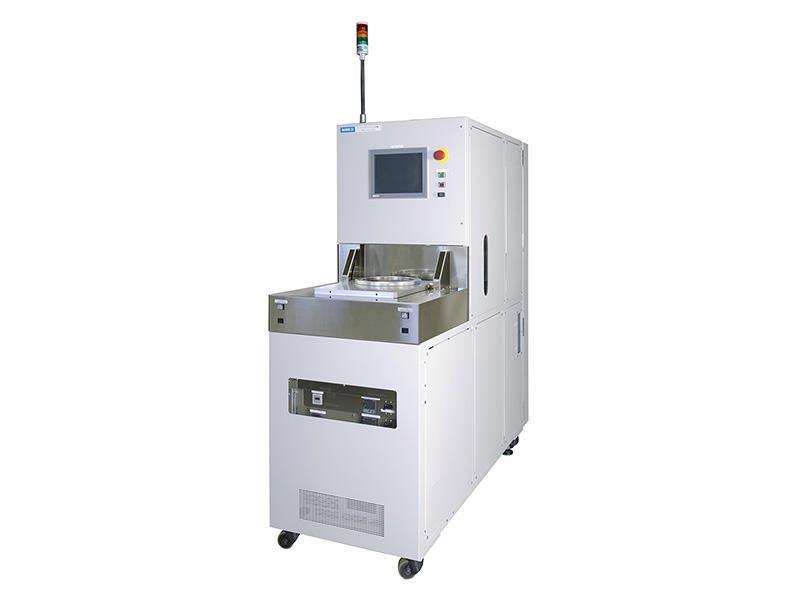
ALD设备 AD-10P
无针孔薄膜沉积
-
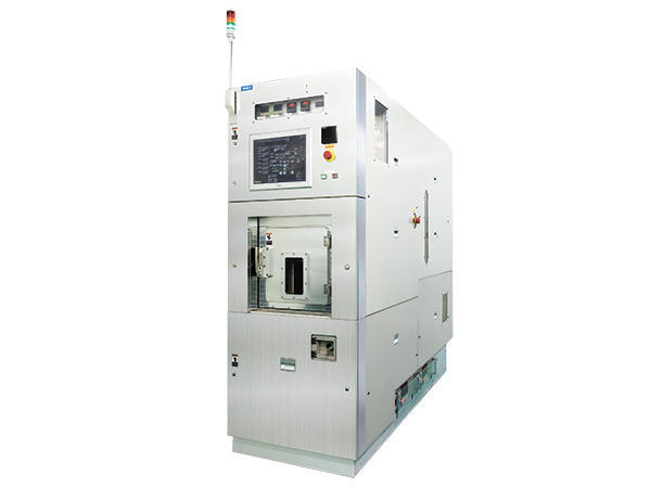
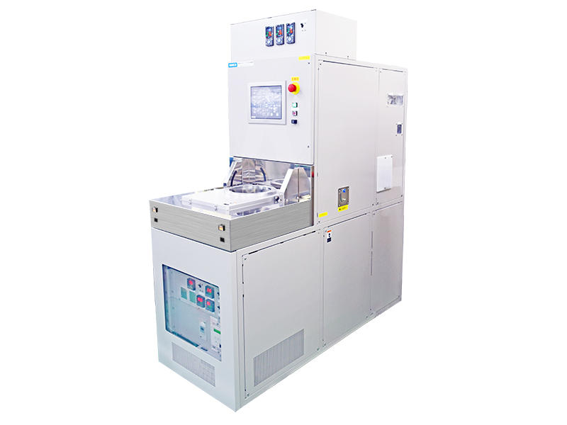
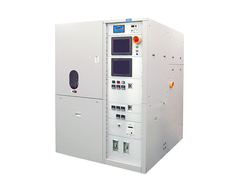
等离子体强化的ALD设备 AD-800LP
卓越的重复性和稳定性


等离子体CVD
等离子体增强化学气相沉积(PECVD)是通过将活性气体变成等离子体状态,在目标基材上产生活性自由基和离子,使目标基材发生化学反应而形成薄膜的技术。在化合物半导体和硅半导体的制造过程中,用于沉积作为钝化膜的氮化硅薄膜(SiN)和作为层间绝缘膜的氧化硅薄膜(SiO₂)。
-
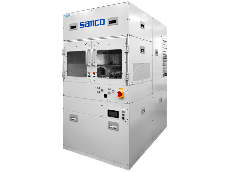
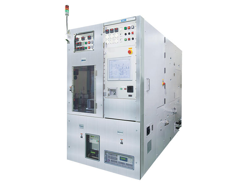
等离子体增强型CVD设备 PD-2201LC
节省空间的生产设备
-
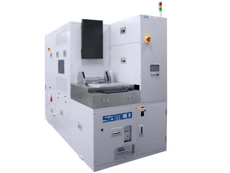
等离子体增强型CVD设备 PD-220NL
紧凑的研发用负载锁定系统
-
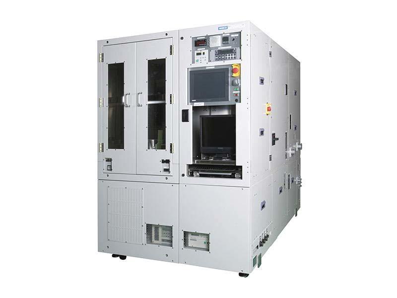
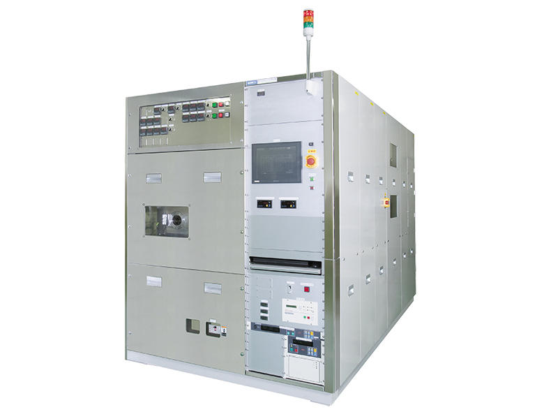
等离子体增强型CVD设备 PD-3800L
基于托盘的批量处理
-
等离子体增强型CVD设备 PD-220N
紧凑的机身,节省空间的设计


液体原料CVD
Samco独特的液态源CVD™系统使用自偏置沉积技术和液态TEOS源来沉积低应力的SiO2薄膜,从薄膜到极厚的薄膜(高达100 µm)。
-
液体原料CVD设备 PD-200STL
负载锁定系统,最高可达200毫米
-
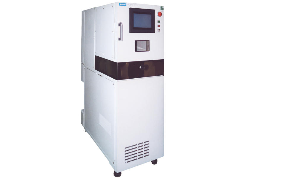
液体原料CVD设备 PD-270STLC
低温厚膜沉积生产设备
-
液体原料CVD设备 PD-330STC
沉积物高达ø300 mm
-
液体原料CVD设备 PD-100ST
开放式研发设备